- 您现在的位置:买卖IC网 > Sheet目录2000 > IDT82V3202NLG (IDT, Integrated Device Technology Inc)IC PLL WAN EBU SGL 68-VFQFPN
IDT82V3202
EBU WAN PLL
Pin Description
14
September 11, 2009
2
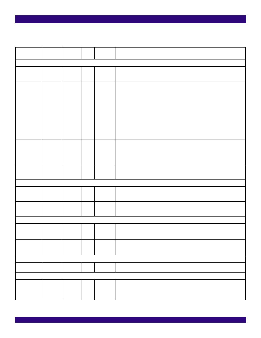
PIN DESCRIPTION
Table 1: Pin Description
Name
Pin No.
(NL68)
Pin No.
(TQFP 64)
I/O
Type
Description 1
Global Control Signal
OSCI
7
6
I
CMOS
OSCI: Crystal Oscillator Master Clock
A nominal 12.8000 MHz clock provided by a crystal oscillator is input on this pin. It is the
master clock for the device.
FF_SRCSW
14
13
I
pull-
down
CMOS
FF_SRCSW: External Fast Selection Enable
During reset, this pin determines the default value of the EXT_SW bit (b4, 0BH) 2. The
EXT_SW bit determines whether the External Fast Selection is enabled.
High: The default value of the EXT_SW bit (b4, 0BH) is ‘1’ (External Fast selection is
enabled);
Low: The default value of the EXT_SW bit (b4, 0BH) is ‘0’ (External Fast selection is dis-
abled).
After reset, this pin selects an input clock for the T0 DPLL if the External Fast selection is
enabled:
High: IN1_CMOS is selected.
Low: IN2_CMOS is selected.
After reset, the input on this pin takes no effect if the External Fast selection is disabled.
SONET/SDH
68
64
I
pull-
down
CMOS
SONET/SDH: SONET / SDH Frequency Selection
During reset, this pin determines the default value of the IN_SONET_SDH bit (b2, 09H):
High: The default value of the IN_SONET_SDH bit is ‘1’ (SONET);
Low: The default value of the IN_SONET_SDH bit is ‘0’ (SDH).
After reset, the value on this pin takes no effect.
RST
51
48
I
pull-up
CMOS
RST: Reset
A low pulse of at least 50 s on this pin resets the device. After this pin is high, the device will
still be held in reset state for 500 ms (typical).
Frame Synchronization Input Signal
EX_SYNC1
30
28
I
pull-
down
CMOS
EX_SYNC1: External Sync Input 1
A 2 kHz, 4 kHz or 8 kHz signal is input on this pin.
EX_SYNC2
35
33
I
pull-
down
CMOS
EX_SYNC2: External Sync Input 2
A 2 kHz, 4 kHz or 8 kHz signal is input on this pin.
Input Clock
IN1_CMOS
31
29
I
pull-
down
CMOS
IN1_CMOS: Input Clock 1
A 2 kHz, 4 kHz, N x 8 kHz 3, 1.544 MHz (SONET) / 2.048 MHz (SDH), 6.48 MHz, 19.44 MHz,
25.92 MHz, 38.88 MHz, 51.84 MHz, 77.76 MHz or 155.52 MHz clock is input on this pin.
IN2_CMOS
32
30
I
pull-
down
CMOS
IN2_CMOS: Input Clock 2
A 2 kHz, 4 kHz, N x 8 kHz 3, 1.544 MHz (SONET) / 2.048 MHz (SDH), 6.48 MHz, 19.44 MHz,
25.92 MHz, 38.88 MHz, 51.84 MHz, 77.76 MHz or 155.52 MHz clock is input on this pin.
Output Frame Synchronization Signal
FRSYNC_8K
18
17
O
CMOS
FRSYNC_8K: 8 kHz Frame Sync Output
An 8 kHz signal is output on this pin.
Output Clock
OUT1_POS
OUT1_NEG
20
21
19
20
O
PECL/LVDS
OUT1_POS / OUT1_NEG: Positive / Negative Output Clock 1
A 1 Hz, 400 Hz, 2 kHz, 8 kHz, 64 kHz, N x E1 4, N x T1 5, N x 13.0 MHz 6, N x 3.84 MHz 7,
E3, T3, 6.48 MHz, 19.44 MHz, 25.92 MHz, 38.88 MHz, 51.84 MHz, 77.76 MHz, 155.52 MHz,
311.04 MHz or 622.08 MHz clock is differentially output on this pair of pins.
发布紧急采购,3分钟左右您将得到回复。
相关PDF资料
IDT82V3255TFG
IC PLL WAN SMC STRATUM 3 64-TQFP
IDT82V3280APFG
IC PLL WAN SE STRATUM 2 100TQFP
IDT82V3285AEQG
IC PLL WAN SE STRATUM 100TQFP
IDT82V3285EQG
IC PLL WAN SE STRATUM 100TQFP
IDT82V3288BCG
IC PLL WAN 3E STRATUM 2 208CABGA
IDT82V3355EDG
IC PLL WAN SYNC ETHERNET 64TQFP
IDT82V3358EDG
IC PLL WAN SYNC ETHERNET 64TQFP
IDTCSPT857DNLG8
IC PLL CLK DVR SDRAM 40-VFQFPN
相关代理商/技术参数
IDT82V3202NLG8
功能描述:IC PLL WAN EBU SGL 68-VFQFPN RoHS:是 类别:集成电路 (IC) >> 时钟/计时 - 专用 系列:- 标准包装:1,500 系列:- 类型:时钟缓冲器/驱动器 PLL:是 主要目的:- 输入:- 输出:- 电路数:- 比率 - 输入:输出:- 差分 - 输入:输出:- 频率 - 最大:- 电源电压:3.3V 工作温度:0°C ~ 70°C 安装类型:表面贴装 封装/外壳:28-SSOP(0.209",5.30mm 宽) 供应商设备封装:28-SSOP 包装:带卷 (TR) 其它名称:93786AFT
IDT82V3202NLGBLANK
制造商:IDT 制造商全称:Integrated Device Technology 功能描述:EBU WAN PLL
IDT82V3255
制造商:IDT 制造商全称:Integrated Device Technology 功能描述:WAN PLL
IDT82V3255_08
制造商:IDT 制造商全称:Integrated Device Technology 功能描述:WAN PLL
IDT82V3255DK
制造商:IDT 制造商全称:Integrated Device Technology 功能描述:WAN PLL
IDT82V3255DKG
功能描述:IC PLL WAN SMC STRATUM 3 64-TQFP RoHS:是 类别:集成电路 (IC) >> 时钟/计时 - 专用 系列:- 标准包装:1,500 系列:- 类型:时钟缓冲器/驱动器 PLL:是 主要目的:- 输入:- 输出:- 电路数:- 比率 - 输入:输出:- 差分 - 输入:输出:- 频率 - 最大:- 电源电压:3.3V 工作温度:0°C ~ 70°C 安装类型:表面贴装 封装/外壳:28-SSOP(0.209",5.30mm 宽) 供应商设备封装:28-SSOP 包装:带卷 (TR) 其它名称:93786AFT
IDT82V3255DKG8
功能描述:IC PLL WAN SMC STRATUM 3 64-TQFP RoHS:是 类别:集成电路 (IC) >> 时钟/计时 - 专用 系列:- 标准包装:1,500 系列:- 类型:时钟缓冲器/驱动器 PLL:是 主要目的:- 输入:- 输出:- 电路数:- 比率 - 输入:输出:- 差分 - 输入:输出:- 频率 - 最大:- 电源电压:3.3V 工作温度:0°C ~ 70°C 安装类型:表面贴装 封装/外壳:28-SSOP(0.209",5.30mm 宽) 供应商设备封装:28-SSOP 包装:带卷 (TR) 其它名称:93786AFT
IDT82V3255EDGBLANK
制造商:IDT 制造商全称:Integrated Device Technology 功能描述:WAN PLL